Table of Contents
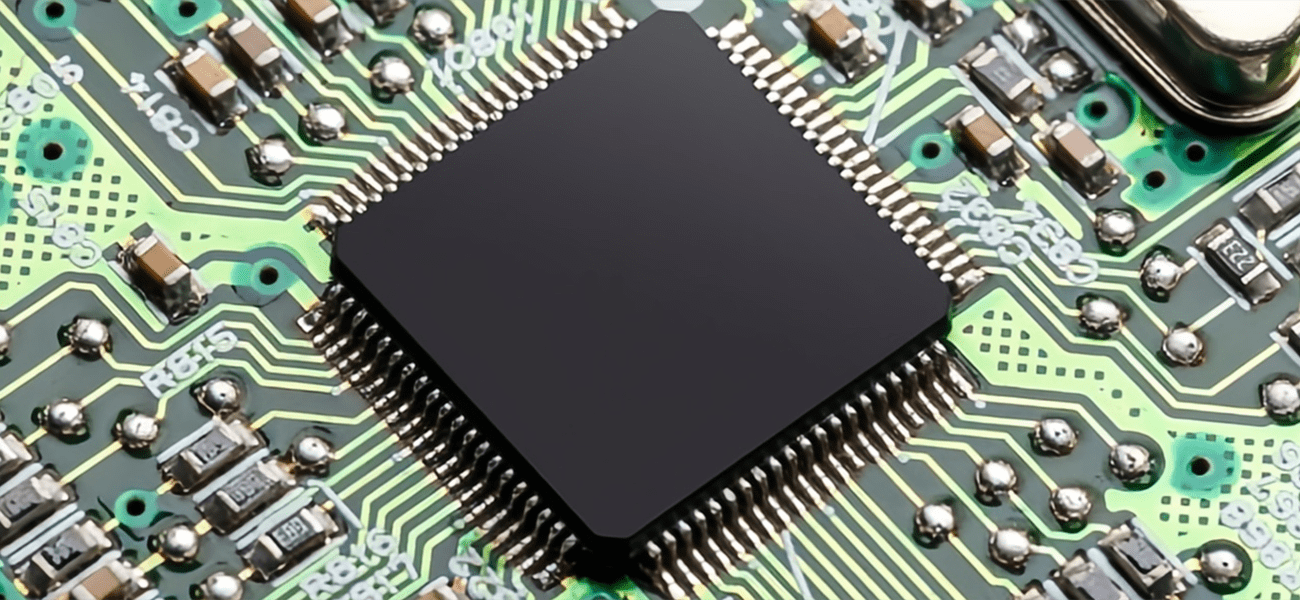
Laser technology is one of the four major inventions of the 20th century, alongside atomic energy, semiconductors, and computers. Over the past 50 years, laser technology has developed rapidly and has been widely applied in various fields, including industrial production, communication, information processing, healthcare, cultural education, and scientific research. As electronic products have evolved towards multifunctionality, portability, and miniaturization, the demands on electronic circuit fabrication have increased.
Laser Processing Goes Mainstream in the Electronics Industry
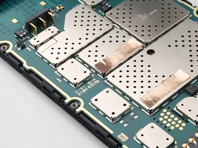
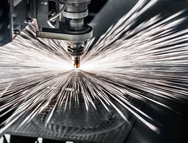
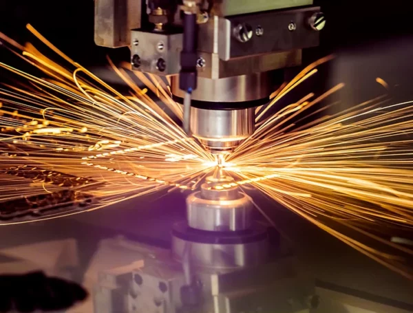
Laser processing utilizes the energy of light focused through lenses to achieve a high energy density at the focal point, allowing for processing through photothermal effects. Laser processing requires no tools, offers high processing speed, minimal surface deformation, and can process a variety of materials. It is a non-contact method, making it ideal for the electronics industry as it avoids mechanical pressure or stress, meeting its processing requirements. Laser processing is widely applied in the electronics industry due to its efficiency, lack of pollution, high precision, and minimal heat-affected zone.
Advantages of Laser Processing in the Electronics Industry
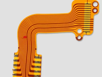
Applications of Laser Equipment in the Electronics Industry
Laser technology encompasses multiple disciplines, including optics, mechanics, electronics, materials, and detection. Its research scope can be categorized into laser processing systems, which include lasers, optical systems, processing machines, control systems, and inspection systems, and laser processing techniques, such as cutting, welding, surface treatment, perforating, marking, and fine adjustment. Laser processing equipment primarily includes laser cutting machines, laser welding machines, and laser marking machines.
Laser Welding Technology in the Electronics Industry
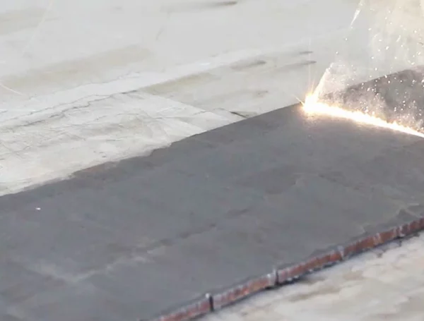
With the demand for smarter electronic products, circuit boards have become smaller, thinner, with more layers and electronic components. Laser welding has seen increasing use in the circuit board industry, especially in microelectronics. Laser welding has a small heat-affected zone, rapid heat concentration, and low thermal stress, making it uniquely advantageous in the packaging of integrated circuits and semiconductor devices. Laser welding is also used in the development of vacuum devices, such as molybdenum-focused electrodes, stainless steel support rings, and fast-heating cathode filament assemblies.
Laser Cutting Technology in the Electronics Industry
Ultraviolet laser cutting has demonstrated significant technological advantages in the separation of circuit boards in the SMT industry and micro-drilling in the PCB industry. Depending on the thickness of the circuit board material, the laser cuts the required contours once or multiple times. Thinner materials allow for faster cutting. Laser cutting provides higher processing quality and efficiency for similar circuit board materials, reducing production costs and expanding the range of product design and processing.
Laser Marking Technology in the Electronics Industry
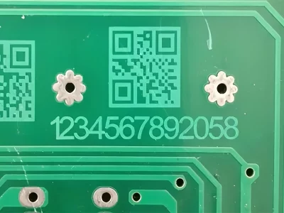
Laser marking technology is one of the most prominent applications of laser processing. Depending on the material characteristics of circuit boards or electronic products, laser marking has extensive applications in the electronics industry. Laser marking involves using high-energy density lasers to locally irradiate the workpiece, causing the surface material to vaporize or undergo a chemical reaction resulting in a permanent mark. Laser marking offers high precision, fast speed, clear marking, and long-lasting effects. In the circuit board production process, it enables better information tracing and can be flexibly applied to various textual information, including complex product logos, QR codes, and more, addressing practical application problems that traditional methods struggle to achieve efficiently.
Laser Technology for Solder Mask Removal
When producing solder masks, issues such as through-hole blockage or misalignment leading to solder pad coverage can occur. Laser technology offers a solution to both problems. By using lasers to penetrate holes blocked by solder mask and then removing the remaining material with a solvent, this process is fast and does not damage the board. Laser technology can quickly and accurately remove solder mask layers from circuit boards.
Laser Technology for Circuit Board Drilling
Laser drilling machines are used for blind hole drilling in HDI and IC carrier boards, and they are the most widely used lasers in the PCB industry, with nearly 20 years of history. As electronic products continue to evolve toward lightweight, thin, short, and small dimensions, the use of HDI technology in circuit boards is increasing. Laser drilling is also applied to flexible boards. As the diameter of through-holes on flexible boards becomes smaller, with production of 0.1 mm diameter holes already underway and further development toward 0.08 mm and 0.05 mm, mechanical drilling costs rise, while laser drilling costs decrease, offering good hole shape and electroplating effects.
YUPEC Advanced Laser Processing Solutions for Electronics Industry
The electronics industry is one of the cores of the global high-tech industry, with its products extensively used in fields such as computers, communications, and consumer electronics. In such a rapidly changing and fiercely competitive industry, YUPEC company, leveraging its advanced laser product line, offers customers efficient and high-precision solutions.
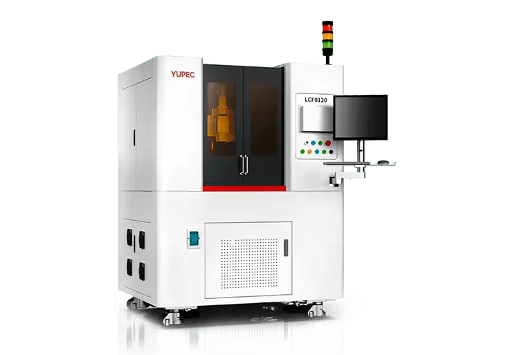
PRECISION FIBER LASER CUTTING MACHINE - LCF0120
The LCF0120 is not only a powerful assistant in the semiconductor industry but also an important tool to drive the technological progress of the industry. It can be applied in the cutting of LED chips and the sorting process of semiconductor wafers. With its outstanding cutting precision and efficiency, it creates higher value for enterprises.
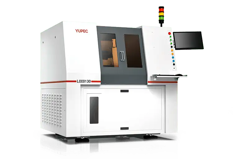
PRECISION CO2 LASER CUTTING MACHINE - LCC0130
The LCC0130 model is a high-precision laser cutting machine designed for processing non-metal materials, widely used in semiconductor packaging and testing stages. Especially when handling micro circuit boards and specialty films, it ensures efficient and precise cutting.
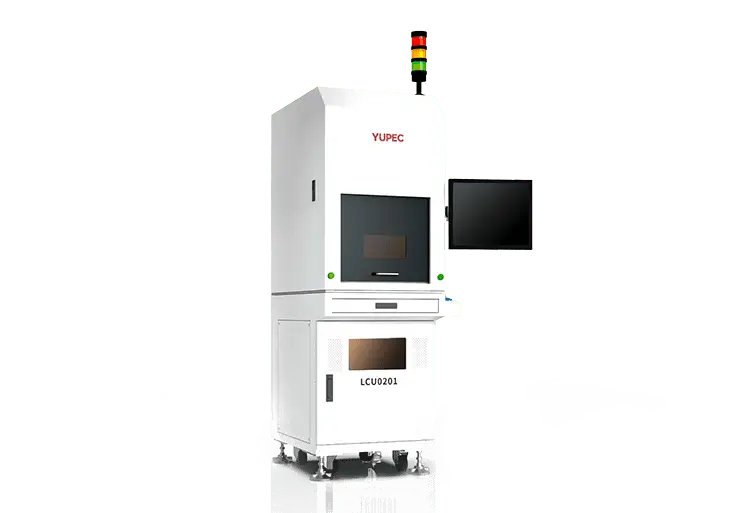
PRECISION UV LASER CUTTING - LCU0201
LCU0201 focuses on providing fine material handling solutions, capable of high-precision cutting of tiny components and thin film materials in the semiconductor production line, thus meeting the semiconductor industry’s strict requirements for precision and efficiency.
APEX SERIES-LASER MICROMACHINING
The APEX series sets a new benchmark in laser micromachining, with its high-speed micro-hole cutting technology widely used in various stages of the semiconductor industry, including the machining of precision parts and the manufacturing of integrated circuits, offering customers fast, precise, and high-quality production solutions.
AXIS SERIES PRECISION CUTTING
The AXIS series offers an efficient and reliable solution for precision laser cutting, fulfilling the diversified needs of modern industry, especially the semiconductor industry, in hardware manufacturing and precision machining of electronic metal plates.
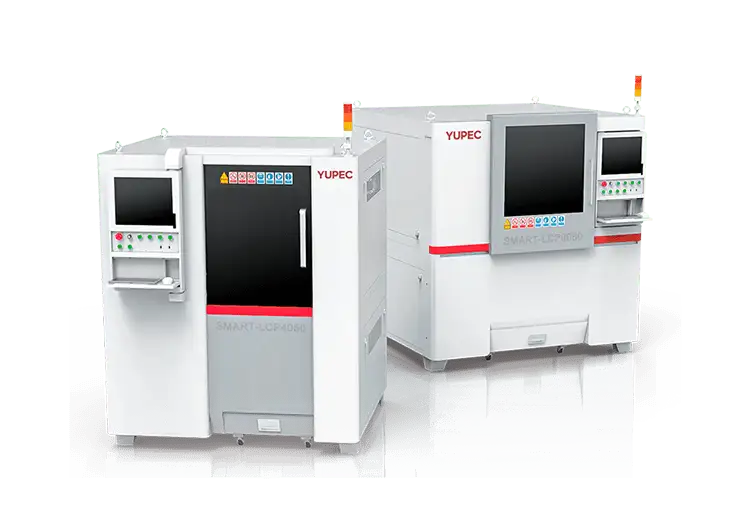
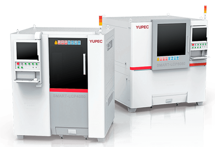
SMART LCP SERIES
The SMART LCP series emphasizes highly precise and stable production processes. Its advanced cooling system and custom accessories can adapt to the high requirements of the semiconductor industry in fine machining and production efficiency.
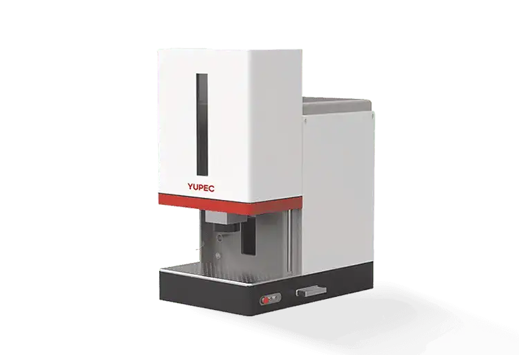
SMART MARKING MACHINE - TECHSCRIBE SERIES
The TechScribe Series is a state-of-the-art laser marking solution tailored to meet the multifaceted demands of contemporary industries. Engineered for precision, speed, and adaptability, this series offers a range of power options and laser sources to suit your specific needs.
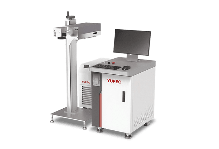
SMART MARKING MACHINE - SPEEDMARK SERIES
The SpeedMark Series offers unparalleled speed and precision in laser marking, making it the go-to choice for high-throughput industrial applications. With a marking speed of up to 12,000 mm/s, this series is designed for rapid, flight marking on the assembly line.
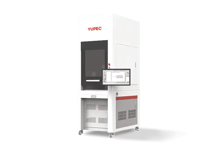
SMART MARKING MACHINE - AUTO-FOCUS SERIES
The Auto-Focus Series is engineered for precision and speed, featuring dynamic focusing technology that allows for superior adaptability in various industrial applications. With a marking speed of up to 7000 mm/s and a focus length of 160mm, this series sets a new standard in laser marking efficiency.
Development of Laser Processing Equipment
Currently, consumer electronics are upgrading toward high precision, thinness, and high integration, with the increasing use of new materials like thin films, hard brittle transparent materials, and special thin metal materials. Laser processing, as a non-contact processing technology with unique advantages such as high efficiency, high precision, low heat effect, and spatial selectivity, is an ideal method for processing these new materials. As technology matures and costs decrease, the laser processing equipment market is expected to experience explosive growth in the coming years.


